
Source: Fair Observer
The Fascinating World of Semiconductors
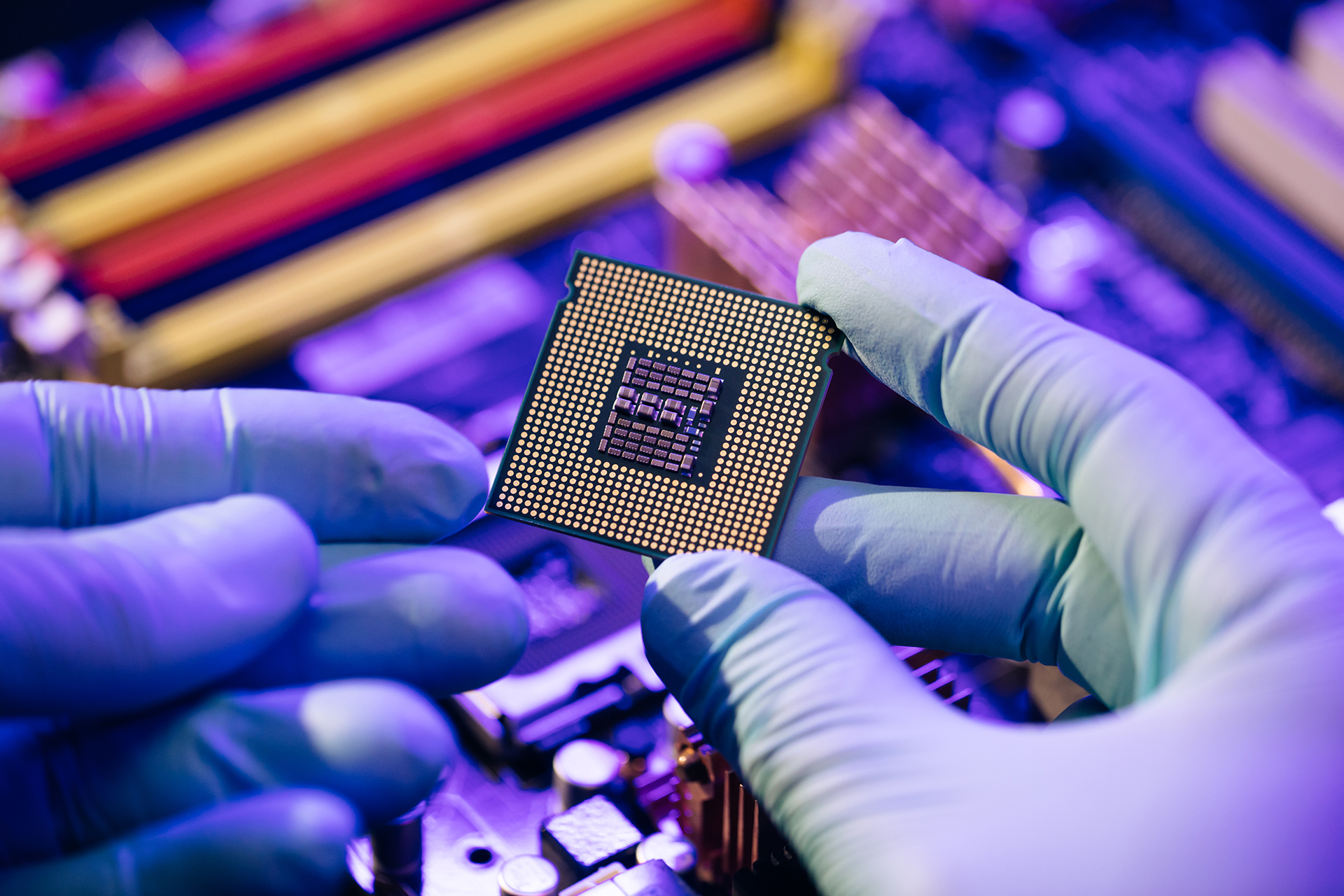
Understanding Semiconductor Conductivity
Semiconductors are versatile materials that owe their wide range of applications to their unique ability to adjust conductivity easily. By introducing minute amounts of impurities called dopants, the conductivity of semiconductors can be altered significantly, sometimes spanning several orders of magnitude. Even with dopant concentrations as low as parts per billion, the material’s conductivity can be dramatically changed. Additionally, applying a voltage or current to one part of the semiconductor can induce a substantial change in conductivity in another part of the device.
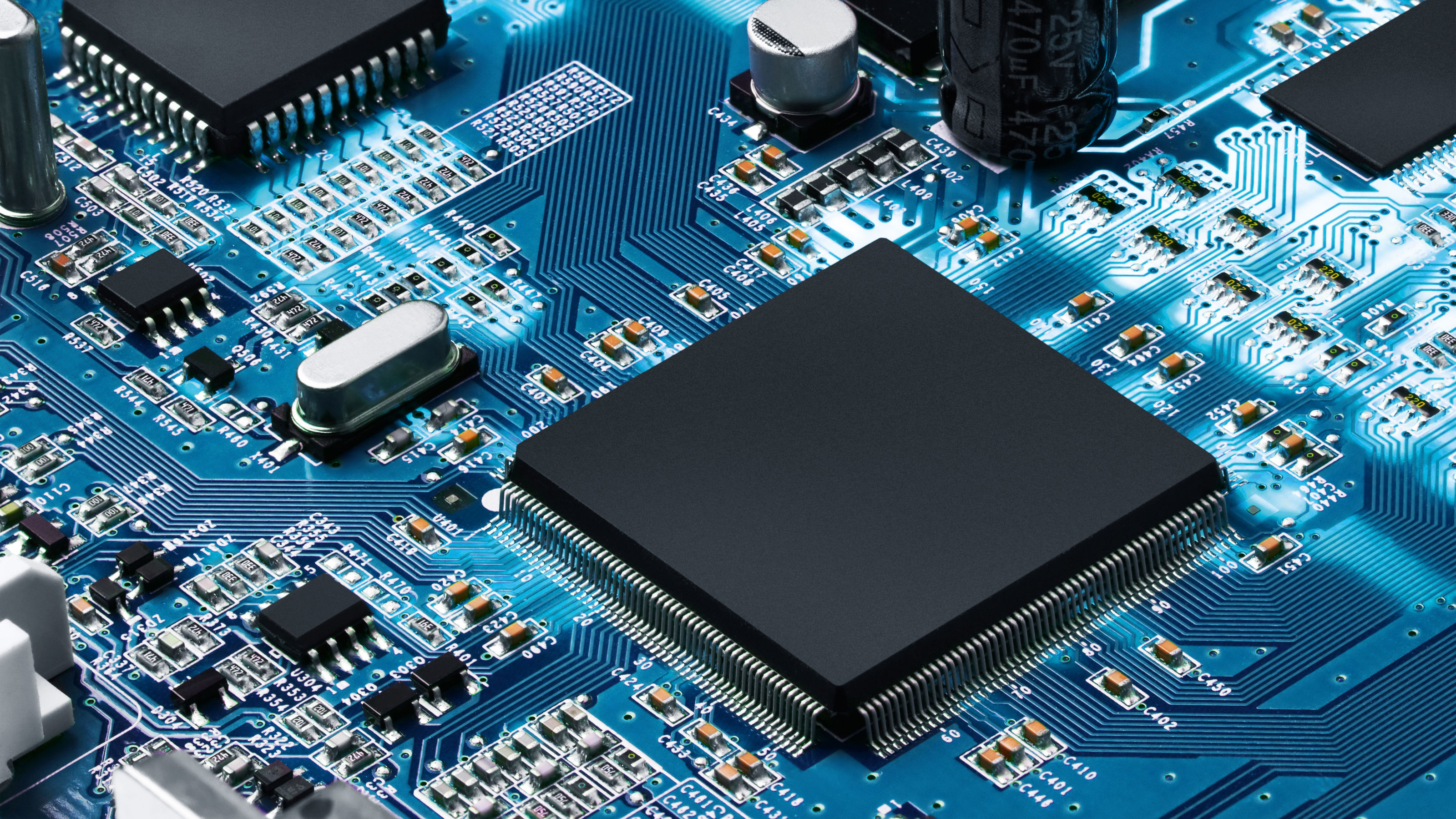
Solar Cells and Semiconductor Devices
Solar cells, a prominent application of semiconductors, are typically constructed using PN junction devices. These cells essentially function as large diodes optimized for light absorption. Solar cells fall under the category of bipolar junction devices, which encompasses diodes and bipolar junction transistors (BJTs).
Unit Systems in Semiconductor Technology
In semiconductor technology, the CGS (centimeter, gram, second) unit system is commonly employed. However, when measuring the thickness of components like solar cells, microns are often used. To simplify modeling and calculations, it is convenient to convert all dimensions to centimeters. For instance, a wafer with a thickness of 160 μm would be equivalent to 0.016 cm.
Understanding the principles of semiconductor conductivity and its applications in devices like solar cells provides a glimpse into the intricate world of semiconductor technology. The ability to manipulate conductivity with precision has paved the way for innovations in various industries, from electronics to renewable energy.
Source: Bosch Rexroth