
Source: Imina Technologies
Scanning Electron Microscope (SEM)
Scanning electron microscope (SEM) images are invaluable for studying the intricate details of solar cells. These images can reveal features that are on the scale of microns, making them impossible to observe with an optical microscope. One significant advantage of an SEM is its superior depth of field, allowing the entire device to be in focus simultaneously, unlike optical microscopes which only focus on specific parts at high magnification.
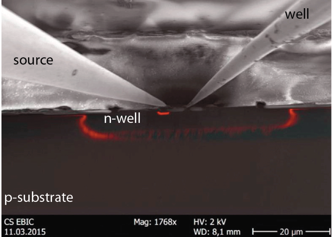
Electron Beam Induced Current (EBIC)
Electron Beam induced current (EBIC) is a technique used to visualize the electrically active regions within a device. By sweeping an electron beam across the sample and measuring the output current, bright regions indicate where electrons are collected by the junction, while dark regions signify uncollected electrons. Combining EBIC images with SEM pictures can provide a clearer depiction of the active areas within the device.
EBIC is not only useful for device analysis but also for material characterization. By adjusting the energy of the electron beam, the depth and volume of electrical excitation can be controlled, aiding in the identification of defects. Sweeping the beam across the device’s surface allows for the detection of electrically inactive areas such as grain boundaries. Analyzing the induced current provides insights into the diffusion length of carriers within the material.
Source: Imina Technologies