Source: SlideServe
Understanding Wide Base Diodes in Solar Cells
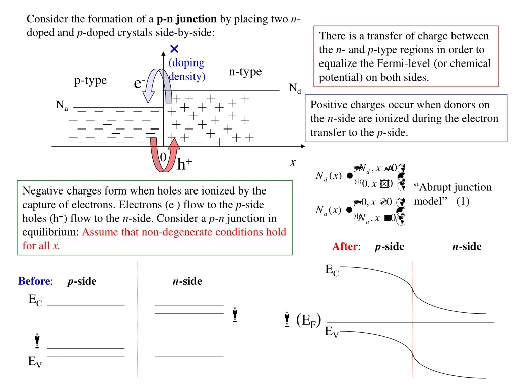
Overview of Wide Base Junction
A wide base junction in a solar cell refers to a situation where the surface of the solar cell is sufficiently far away from the junction edges. This positioning ensures that the recombination properties of carriers injected into the quasi-neutral region (QNR) under forward bias are not influenced.
Solving for Carrier Concentrations
In the wide base diode scenario, the solution involves determining carrier concentrations and currents in the quasi-neutral regions. This process includes finding the general solution for both n-type and p-type materials. By considering low injection recombination and constant generation, the differential equations can be derived and solved accordingly.
Particular Solution for Wide Base Diode
To find the particular solution for a wide base diode, boundary conditions at the edge of the depletion region are crucial. These conditions ensure that the minority carrier concentration remains finite even as x tends to infinity. By setting the appropriate parameters, such as B = 0, the general solutions for both holes and electrons can be derived.
Finding Total Current
Calculating the total current in a wide base diode involves understanding the current changes across the depletion region. By considering factors such as generation and recombination, the total current can be determined using relevant equations for both n-type and p-type materials.
In conclusion, the analysis of wide base diodes in solar cells is essential for understanding the behavior of carriers and currents in different regions of the device. By following the steps outlined above, researchers and engineers can gain valuable insights into the performance of solar cells with wide base junctions.

Source: SlidePlayer
